lead iodide(PbI2) residue on the performance of perovskite solar cells
Perovskite solar cells (PSCs) have rapidly emerged as a revolutionary technology in the photovoltaic landscape, boasting impressive power conversion efficiencies that now rival conventional silicon. A seemingly minor detail in their fabrication, the presence of lead iodide (PbI2) residue within the perovskite film, has surprisingly become a central topic of debate and research. While often considered an impurity, the role of unreacted PbI2 is far more nuanced, acting as a double-edged sword that can either enhance initial device performance or severely compromise long-term stability. This article will delve into the complex interplay between PbI2 residue and the overall characteristics of perovskite solar cells, examining its origins, its positive and negative impacts, and the ongoing strategies to manage its presence for optimal device efficiency and stability.
Solar energy, as a clean source of energy, is currently one of the best solutions to the energy crisis. Perovskite solar cells are a popular area of research. Lead iodide is an important material for new perovskite batteries.
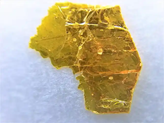
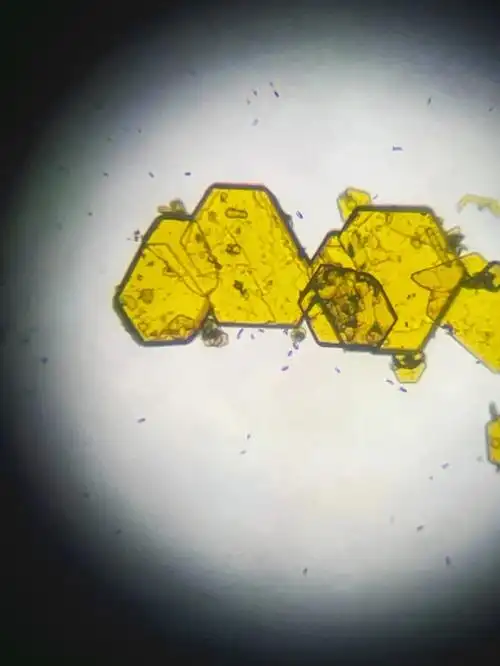
Chongqing Yuhan Technology Co., Ltd. offers ultra-pure lead iodide. This material has good solubility and leaves less residue. These qualities can enhance the performance of perovskite solar cell devices。
Introduction: The Perovskite Promise and the PbI2 Enigma
- Hook: Start with the rapid rise of perovskite solar cells and their impressive potential to revolutionize solar energy, highlighting their record efficiencies.
- Problem/Enigma: Introduce the seemingly paradoxical role of lead iodide (PbI2) residue – initially perceived as a detrimental impurity, but now understood to exert complex, multifaceted effects on PSC performance.
- Article’s Purpose: Clearly state the article’s aim to explore how PbI2 residue influences perovskite solar cell performance, covering both its beneficial contributions and its detrimental drawbacks, and outlining current strategies for its strategic management and optimization.
What is Lead Iodide (PbI2) Residue in Perovskite Solar Cells?
- Definition: Explain that PbI2 residue (also often called residual PbI2 or unreacted PbI2) refers to the lead iodide precursor material that remains in the perovskite active layer after the film synthesis process.
- Formation Mechanisms: Detail the common ways PbI2 residue ends up in the final perovskite film:
- Incomplete Conversion: This is the primary mechanism, particularly in two-step fabrication methods. PbI2 is initially deposited as a film, and then reacted with an organic ammonium halide (e.g., methylammonium iodide, MAI, or formamidinium iodide, FAI). If the reaction is incomplete, excess PbI2 remains.
- Perovskite Degradation: Under prolonged stress conditions (e.g., high heat, excessive humidity, intense light exposure), the perovskite material (like MAPbI3) can partially decompose back into its constituent precursors, including PbI2. This forms PbI2 in situ.
- Intentional Excess Precursor: In some one-step deposition methods, a slight excess of PbI2 is intentionally added to the precursor solution. This strategy is employed to control crystallization kinetics or promote certain beneficial effects (discussed later).
The “Good” Side: Beneficial Effects of Controlled PbI2 Residue
Highlight the positive impacts when PbI2 is present in controlled, optimal amounts.
- Defect Passivation at Interfaces and Grain Boundaries:
- Mechanism: Explain how a judicious amount of PbI2 tends to preferentially segregate to the interfaces between the perovskite layer and the charge transport layers (ETL/HTL) or at the grain boundaries within the perovskite film itself.
- Electronic Role: PbI2 has a wider bandgap (around 2.3 eV) compared to typical perovskites (e.g., MAPbI3 ~1.6 eV). This difference can create a favorable Type I heterojunction at these interfaces. This energetic alignment can effectively “passivate” or neutralize detrimental surface defects (e.g., lead vacancies, iodine interstitials) that act as non-radiative charge recombination centers.
- Impact on Performance: This passivation leads to:
- Higher Open-Circuit Voltage (Voc), as fewer carriers recombine non-radiatively.
- Improved Fill Factor (FF), indicating better charge collection efficiency.
- Enhanced overall Power Conversion Efficiency (PCE).
- Improved Crystallization and Film Morphology:
- Templating Effect: Small amounts of PbI2 can act as a template or scaffold, guiding the growth of larger, more uniform, and highly crystalline perovskite grains. This can reduce the formation of undesirable smaller grains and amorphous regions.
- Reduced Pinholes and Improved Density: A well-controlled presence of PbI2 can help fill in microscopic pinholes or improve the overall density and compactness of the perovskite film. This leads to better coverage, reduces shunt paths, and improves carrier transport.
- Facilitated Charge Extraction (Interface Engineering):
- Barrier Effect: PbI2 at perovskite/charge transport layer interfaces can sometimes create a shallow energy barrier that helps repel minority carriers (e.g., holes at the ETL interface), effectively guiding majority carriers towards their respective transport layers and reducing interfacial recombination.

The “Bad” Side: Detrimental Effects of Excess or Uncontrolled PbI2 Residue
Discuss the negative consequences when PbI2 is present in excessive or unmanaged amounts.
- Increased Charge Recombination (if not passivating):
- Mechanism: If PbI2 exists as bulk impurities or large domains, rather than precisely localized passivation layers, it can act as its own defect site or create detrimental interfaces that lead to non-radiative charge recombination.
- Impact on Performance: This results in:
- Lower Voc due to increased non-radiative pathways.
- Reduced FF due to poor charge collection.
- Overall drop in PCE.
- Device Hysteresis:
- Mechanism: Excess PbI2 (especially at interfaces) can contribute to ion migration (e.g., I⁻) or create trap states that lead to slow trapping/de-trapping kinetics.
- Impact: This manifests as prominent current-voltage (J-V) hysteresis, where the measured efficiency varies significantly depending on the scan direction, making device performance difficult to quantify accurately.
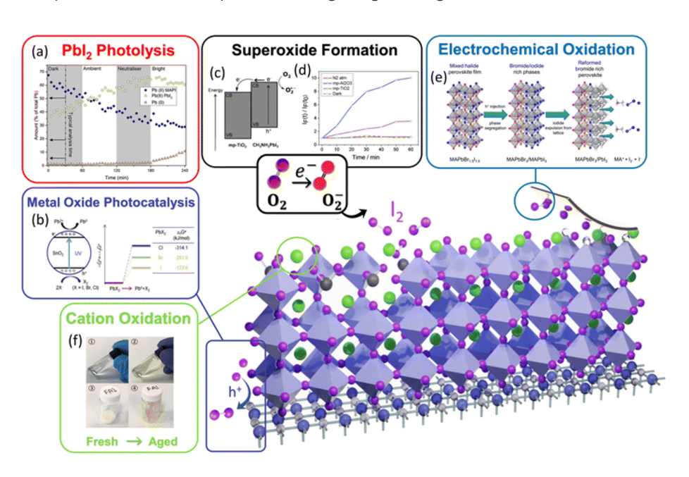
- Degradation Pathway and Reduced Stability:
- Moisture Ingress: Bulk PbI2 is highly susceptible to moisture. Its presence provides pathways for water ingress into the perovskite layer, accelerating the decomposition of the perovskite material.
- Photodegradation: While perovskite itself can be light-sensitive, the presence of PbI2 can exacerbate photodegradation, especially under humid conditions, acting as a catalyst for decomposition.
- Volume Changes: Phase transitions or hydration of PbI2 can lead to volume changes that stress the perovskite film, causing cracks and delamination.
- Impact: Significantly reduced long-term stability under environmental stress (heat, humidity, light), limiting practical application.
- Poor Film Quality:
- Morphological Defects: Large, unreacted PbI2 domains can lead to rougher films, more pinholes, and uneven morphology, creating shunting paths and reducing device performance.
- Scattering Losses: Large PbI2 precipitates can cause light scattering within the active layer, reducing the amount of light absorbed by the perovskite and thus lowering the photocurrent (Jsc).
Strategies for Managing PbI2 Residue: Towards Optimal PSC Performance
Discuss various approaches researchers employ to control and optimize the amount and location of PbI2 residue.
- Fabrication Method Optimization:
- Solvent Engineering: Using specific solvent additives or solvent combinations (e.g., DMSO, DMF, GBL) to control PbI2 solubility and reaction kinetics.
- Antisolvent Treatment: Precise timing and choice of antisolvents (e.g., chlorobenzene, toluene) to induce rapid crystallization and minimize PbI2 residue.
- Vapor-Assisted Deposition: Offers better control over precursor reaction and film formation.
- Annealing Conditions: Optimizing annealing temperature and time to ensure complete conversion without inducing degradation.
- Additive Engineering:
- Excess PbI2 Strategy: Carefully controlling the intentional addition of a small excess of PbI2 to leverage its beneficial passivation effects while avoiding detrimental bulk impurities.
- Other Passivation Additives: Using organic molecules (e.g., phenylethylammonium iodide, PEAI) or inorganic compounds that can passivate defects, often reducing the need for PbI2 residue or working synergistically with it.
- Interface Engineering:
- Modifying Transport Layers: Designing ETLs and HTLs that reduce the accumulation of detrimental PbI2 at their interfaces, or that help to effectively passivate any residual PbI2 layers.
- Surface Treatment: Post-treatment of the perovskite film surface to modify or remove unwanted PbI2 or to create a more stable passivation layer.
- Characterization Techniques:
- Advanced Microscopy (SEM, TEM): To visualize PbI2 distribution and morphology.
- X-ray Diffraction (XRD): To quantify the presence of crystalline PbI2.
- Photoluminescence (PL) Spectroscopy: To assess defect density and recombination pathways.
- Electrochemical Impedance Spectroscopy (EIS): To understand charge transfer and recombination kinetics.
Conclusion: The Delicate Balance of PbI2 in Perovskite Solar Cells
- Recap: Reiterate that lead iodide (PbI2) residue is a complex factor in perovskite solar cells, acting as a double-edged sword.
- Balance: Emphasize the critical need to strike a delicate balance in its presence – leveraging its beneficial passivation and crystallization effects while rigorously avoiding detrimental excess or uncontrolled degradation pathways.
- Future Outlook: Highlight that ongoing research in fabrication, additive engineering, and interface engineering aims to precisely control PbI2 distribution to further boost efficiency and, crucially, enhance the long-term stability of perovskite solar cells, paving the way for their successful commercialization.